With ARM64 a given, Intel has been looking to increase market penetration through chip customization. June 8th Intel revealed plans to manufacture a new (as yet unnamed) server Xeon chip that contains an integrated FPGA. The FPGA and CPU will have coherent access to memory. The combination chip will be package compatible with the existing Xeon E5 line. Intel mentions that FPGAs can deliver “up to 10x” the performance on unspecified industry benchmarks and further claims its implementation will deliver another 2x improvement (so 20x total) because of coherency and lower CPU-FPGA latency.
Essentially the Xeon + FPGA chip package sandwiches an FPGA on top of a Xeon chip and links the two via a Quick Path Interconnect. Such chip packaging is designed to attract enterprise customers looking to minimize latency and maximize performance per watt.
There appears to be justification for this hybrid architecture to overcome (1) initial design costs and (2) vendor lock-in as indicated by the Microsoft ISCA paper about the use of FPGAs in datacenters for page rank processing inside Bing. Succinctly, Microsoft reported up to 95% more throughput for only 10% more power fror an increased total cost of ownership (TCO) of less than 30%.
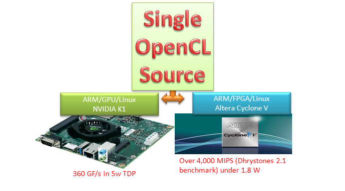
For more information about experimenting with FPGAs and to make your own power/performance evaluation, check out the techEnablement article on the $179 Altera FPGA + ARM evaluation board.
Enterprise Tech reports the Intel stacked FPGA product has been expected for some time:
Even before new management took the helm at Intel last year, the chip maker was looking for ways to leverage its substantial lead in chip manufacturing technology, and Intel formed a partnership with Altera, one of the two suppliers of FPGAs, to allow the latter to use Intel as a foundry for its Stratix line of FPGAs. In late March, Intel and Altera extended their partnership to include the development of multi-die, 3D-stacked devices, so the signals were out there that something like the hybrid Xeon-FPGA chip would be coming along. Under the revised deal announced in March between the two companies, the Stratix 10 FPGAs will be etched using Intel’s 14 nanometer Tri-Gate processes, which incidentally line up with the processes that Intel will be using its current 22 nanometer Tri-Gate processes to make the “Haswell” line of Xeon E5 processors, which are widely expected to come out before the end of the year, and “Broadwell” Xeon E5 chips will not be expected for at least a year after that – and perhaps more. The point is, on such hybrid devices, the processes used to make the two chips do not have to be the same and they can advance at their own paces.
Leave a Reply